蓝宝石基氮化镓功率器件外延片
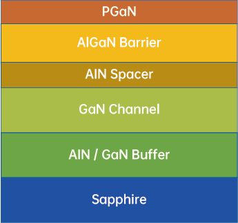
JGETLBX-L4/6
- 4-inch and 6-inch available
- Buffer breakdown voltage > 650V
- Edge cracks < 3mm
- Customized AlGaN and pGaN layer
- High repeatability and good uniformity
| Parameter | SPEC | Measurement technique/tool/conditions | Comments |
| Substrate | |||
| Thickness (um) | 1000 | Micrometer | |
| Flat length (mm) | 47.5 | / | |
| Bevel design | C-M 0.2° | / | |
| Wafer bow | ≤20 um | Stress Mapper | |
| Epi | |||
| EPI total thickness (um) | 2~4 | PL | Base on request |
| Finished 650V EPI wafer bow (6inch) in um | ≤±35 | Stress Mapper | |
| EPI surface rms roughness (AFM, indicate scan size in um2) | ≤1 nm in 5×5 um2 | AFM | |
| Capping layer thickness (nm) | / | TEM | GaN cap :3nm SiN cap:3~100nm |
| pGaN layer thickness (nm) | 100±10 | TEM | Base on request |
| Mg chemical concentration (at/cm3) PCOR-SIMS | 3E+19&4E+19 | PCOR-SIMS | E-mode |
| Mg/H in pGaN(a.u.) PCOR-SIMS | >=2 | PCOR-SIMS | E-mode |
| AlGaN barrier Al percentage | 0.18 | PL | Base on request |
| AlGaN barrier thickness (nm) | 15 | TEM | Base on request |
| AlN spacer thickness (nm) | 0.5 | / | Base on request |
| GaN FWHM (102) | <500 arcsec | XRD | |
| GaN FWHM (002) | <400 arcsec | XRD | |
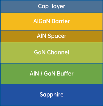
JGDTLBX-L4/6
- 4-inch and 6-inch available
- Buffer breakdown voltage > 650V
- Edge cracks < 3mm
- Customized AlGaN layer
- In-situ Si3N4 or GaN cap layer can be choose
- High repeatability and good uniformity
| Parameter | SPEC | Measurement technique/tool/conditions | Comments |
| Substrate | |||
| Thickness (um) | 1000 | Micrometer | |
| Flat length (mm) | 47.5 | / | |
| Bevel design | C-M 0.2° | / | |
| Wafer bow | ≤20 um | Stress Mapper | |
| Epi | |||
| EPI total thickness (um) | 2~4 | PL | Base on request |
| Finished 650V EPI wafer bow (6inch) in um | ≤±35 | Stress Mapper | |
| EPI surface rms roughness (AFM, indicate scan size in um2) | ≤1 nm in 5×5 um2 | AFM | |
| Cap layer thickness (nm) | / | TEM | GaN cap :3nm SiN cap:3~100nm |
| AlGaN barrier Al percentage | 0.25 | PL | Base on request |
| AlGaN barrier thickness (nm) | 25 | TEM | Base on request |
| AlN spacer thickness (nm) | 1.0 | / | Base on request |
| GaN FWHM (102) | <500 arcsec | XRD | |
| GaN FWHM (002) | <400 arcsec | XRD | |
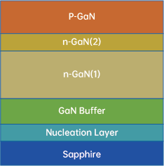
JGXTVBX-L4/6/8
- 4-inch/6-inch/8-inch available
- Buffer breakdown voltage > 750V(based on request)
- Edge cracks < 3mm
- Customized GaN growth layer thickness
- Low warpage and high repeatability
| Parameter | SPEC | Measurement technique/tool/conditions | Comments |
| Substrate | |||
| Thickness (um) | 1000 | Micrometer | |
| Flat length (mm) | 47.5 | / | |
| Bevel design | C-M 0.2° | / | |
| Wafer bow | ≤10 um | Stress Mapper | |
| Epi | |||
| EPI total thickness (um) | >14 | PL | Base on request |
| Finished 1200V EPI wafer bow (6inch) in um | ≤±35 | Stress Mapper | |
| EPI surface rms roughness (AFM, indicate scan size in um2) | ≤0.5 nm in 5×5 um2 | AFM | |
| n-GaN(1)_Si chemical concentration (at/cm3) PCOR-SIMS | 5E+18 | PCOR-SIMS | Base on request |
| n-GaN(2)_Si chemical concentration (at/cm3) PCOR-SIMS | 2~3E+16 | PCOR-SIMS | Base on request |
| Mg chemical concentration (at/cm3) PCOR-SIMS | 3E+19 | PCOR-SIMS | Base on request |
| Mg/H in pGaN(a.u.) PCOR-SIMS | >=2 | PCOR-SIMS | |
| GaN FWHM (102) | <400 arcsec | XRD | |
| GaN FWHM (002) | <300 arcsec | XRD | |