硅基氮化镓功率器件外延片
JGETLBX-S6
- Buffer breakdown voltage > 650V
- Customized AlGaN and pGaN layer
- High repeatability and good uniformity
| Parameter | SPEC | Measurement technique/tool/conditions |
| Epi Measurement | ||
| EPI total thickness (um) | >5 | PL |
| Finished 650V EPI wafer bow (6inch) in um | ≤±35 | Stress Mapper |
| EPI surface rms roughness (AFM, indicate scan size in um2) | ≤1 nm in 5×5 um2 | AFM |
| pGaN layer thickness (nm) | 80±10 | TEM |
| Mg chemical concentration (at/cm3) PCOR-SIMS | 4E+19 | PCOR-SIMS |
| Mg/H in pGaN(a.u.) PCOR-SIMS | >=2 | PCOR-SIMS |
| AlGaN barrier Al percentage | 0.18 | PL |
| AlGaN barrier thickness (nm) | 15 | TEM |
| AlN Spacer thickness(nm) | 0.5 | TEM |
| GaN FWHM (102) | <1600 arcsec | XRD |
| GaN FWHM (002) | <1000 arcsec | XRD |
| Buffer breakdown(150°C)leakage current @1e-5A/mm2 | >650V | / |
| Vth/V | 1.5 | / |
| Ron/Ω·mm | <12 | / |
| Hall Measurement on D-Mode Sample | ||
| 2DEG Sheet resistance (Ω/sq) | 367 | From D-Mode |
| 2DEG Carrier density (/ cm-2) | 9.2E+12 | From D-Mode |
| 2DEG Electron Mobility (cm2/Vs) | 1897 | From D-Mode |

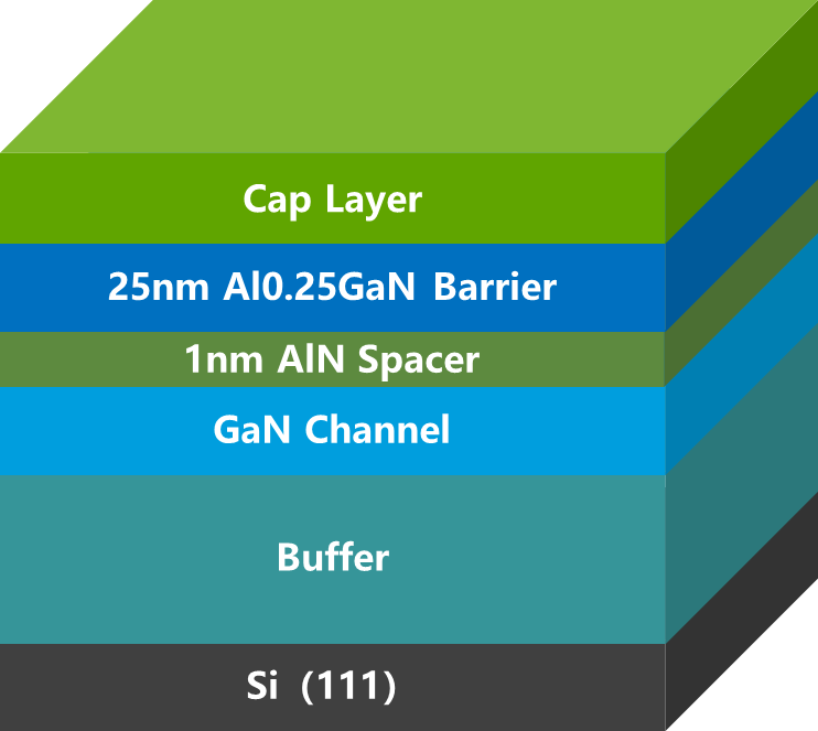
JGDTLBX-S6
- Buffer breakdown voltage > 650V
- Customized AlGaN layer
- In-situ SiN or GaN cap layer can be choose
- High repeatability and good uniformity
| Parameter | SPEC | Measurement technique/tool/conditions |
| Epi Measurement | ||
| EPI total thickness (um) | >5 | PL |
| Finished 650V EPI wafer bow (6inch) in um | ≤±35 | Stress Mapper |
| EPI surface rms roughness (AFM, indicate scan size in um2) | ≤1 nm in 5×5 um2 | AFM |
| Capping layer thickness (nm) | GaN cap :3nm SiN cap:3~100nm | TEM |
| AlGaN barrier Al percentage | 0.25 | PL |
| AlGaN barrier thickness (nm) | 25 | TEM |
| AlN Spacer thickness(nm) | 1 | TEM |
| GaN FWHM (102) | <1600 arcsec | XRD |
| GaN FWHM (002) | <1000 arcsec | XRD |
| Buffer breakdown(150°C)leakage current @1e-5A/mm2 | >650V | / |
| Hall Measurement | ||
| 2DEG Sheet resistance (Ω/sq) | 367 | / |
| 2DEG Carrier density (/ cm-2) | 9.2E+12 | / |
| 2DEG Electron Mobility (cm2/Vs) | 1897 | / |